![]()

")
What are the services provided by SAOM-Lab?
We strive to create solutions to technological problems in the industry as well as the academic fields. SAOM-Lab offers highly specialized services which can be tailored to your own particular needs. Our team of experts will be there to guide you in every step of the way, designing and implementing methodologies or even assisting you in the creation of a new product. Please contact us and describe to us any questions or concerns you may have, we will be happy to help you get started.
Thin film deposition and nanomaterial synthesis
SAOM-Lab performs the design and manufacturing of thin films with optical applications, thus providing functional prototypes that can be fabricated in a mass scale. Among the different coatings we developed are anti-reflection, low-e, protective coatings, interference filters, among others.
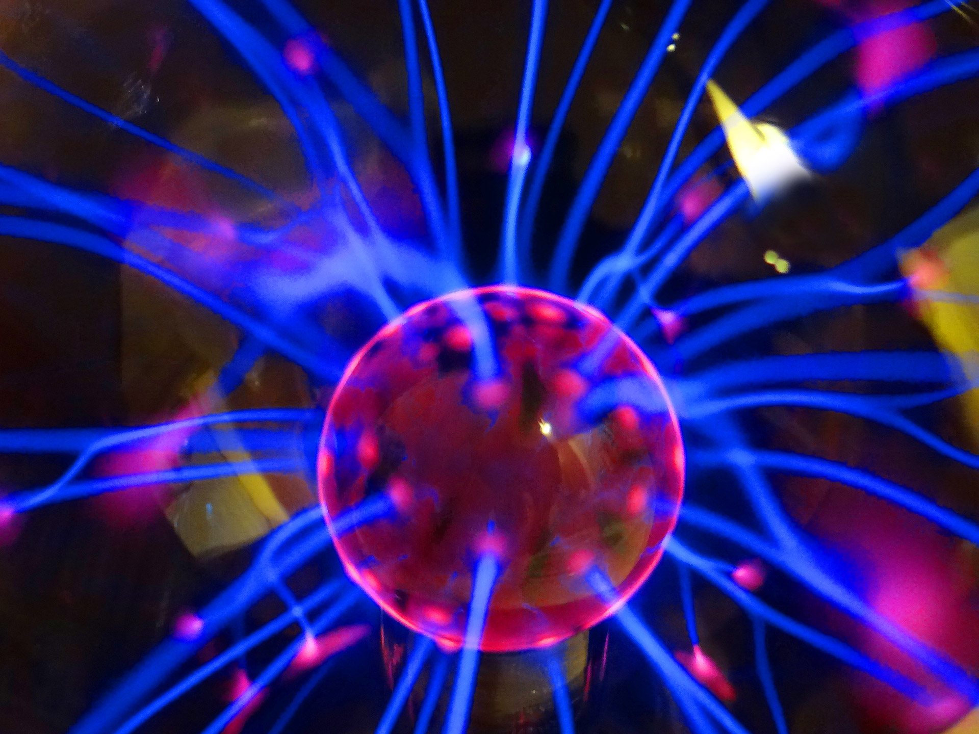
Sputtering
The objective is to combine different materials possessing certain traits and obtaining a new material that interacts with light in a desired way. This is possible by extracting atoms from a material, known as a target, and deposited onto a substrate forming a layer on the substrate's surface. This can be repeated many times until the optimal number of layers is obtained. All the layers form what is known as a thin film, which is actually a material possessing the expected response.
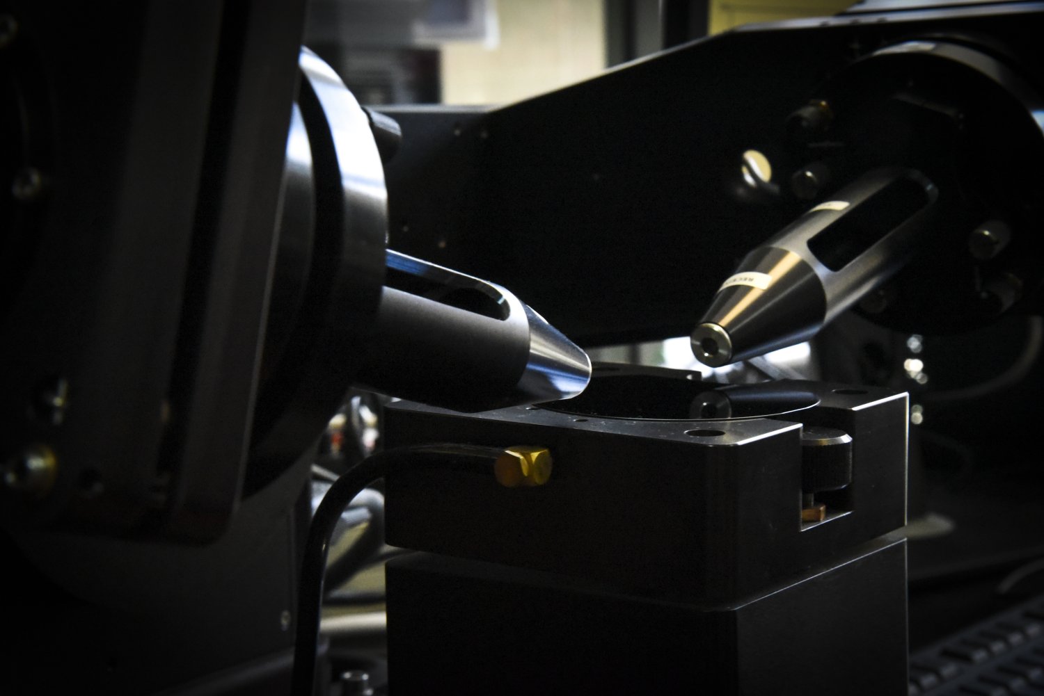
Laser Ablation
Laser ablation is the process of removing material from a sample by focusing an intense pulsed laser beam on it. The employed laser systems usually emit from the near infrared to the near ultraviolet region of the electromagnetic spectrum; they need to have pulse durations of a few nanoseconds to deliver power of a few GWatts per squared centimiter.
Advanced material analysis and characterization
If you wish to have a better control of manufacturing processes, SAOM-Lab's team can assist you in the qualitative and quantitative characterization of raw materials that may be of use to you in your field of work. We use state of the art technology to generate the desired material's metrology.
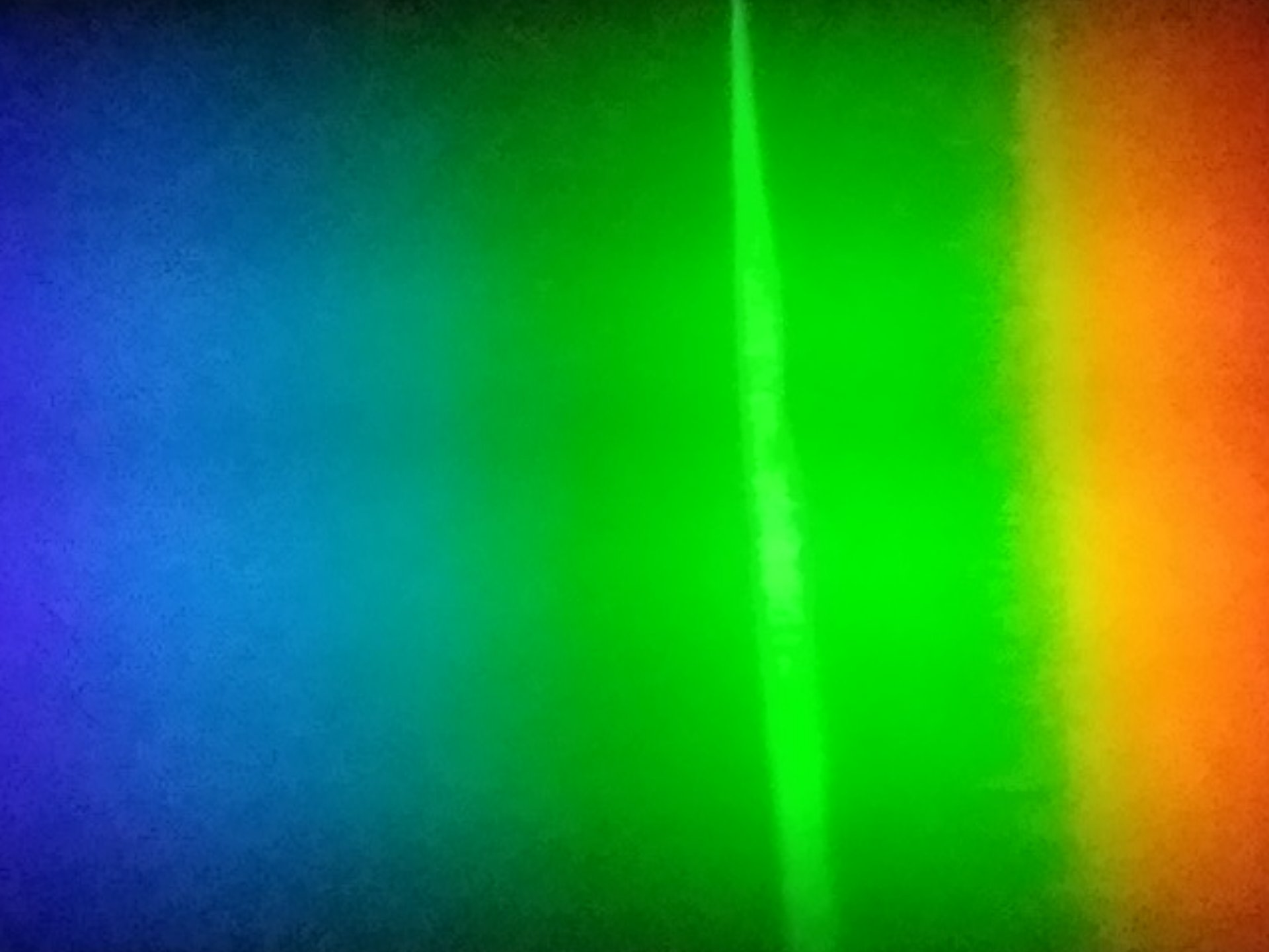
Spectroscopy
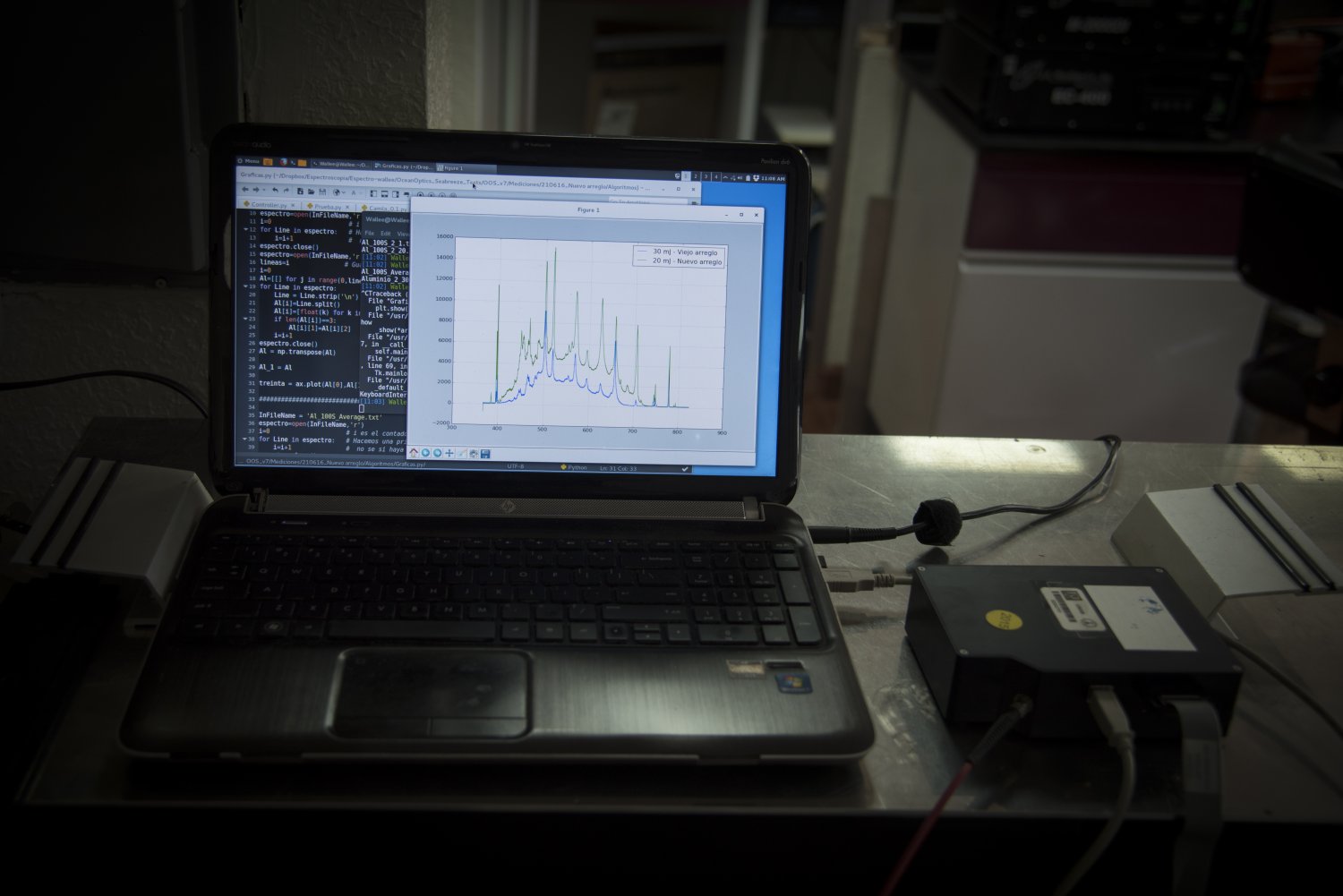
If the light emitted by an object passes through a prism it is separated into a set of colors. All this colors are indeed a measurement of radiation intensity as a function of wavelength and forms what is known as electromagnetic spectrum. If we regard chemical elements in the periodic table we will find a unique set of colors for each element.
Ellipsometry
Ellipsometry is a technique utilized to analyze the optical properties of thin films such as its composition, dielectric permittivity, and the material's layer's thickness.
AFM
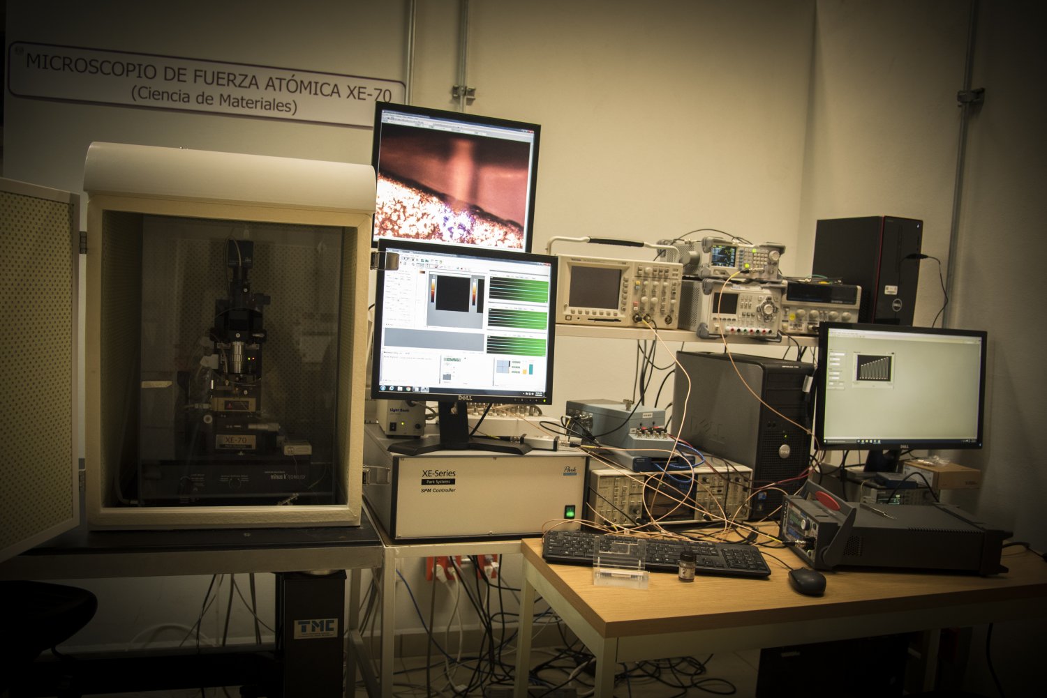
Atomic Force Microscopy (AFM) is a technique used to obtain the physical properties of surfaces at a nanometric level, such as: roughness , elastic properties, friction, and piezo- ferro-electricity. Actually, this technique allows to obtain a 3D topography of a sample's surface. More in practice, AFM consists of a mechanical arm which has a very small pyramid shaped tip called a cantilever which is dragged across the sample's surface.
Technology Consulting
At SAOM-Lab we combine our scientific knowledge with our vast experience in the nanomaterial field mainly oriented to optical applications. Thereby we offer a range of services such as process analysis, issue identification and betterment, lastly, we can assist you with the complete development of turnkey solutions.
Courses and counseling

At SAOM-Lab we share our expertise with our clients by teaching highly specialized courses in the field of nanoscience and nanomaterials.
Contact us
Phone
(+52) 646-1750650. Ext: 433, 382.
info@saomlab.com
Address
CNyN-UNAM Carretera Tijuana-Ensenada Km. 107, Pedregal Playitas, 22860 Ensenada, B.C.
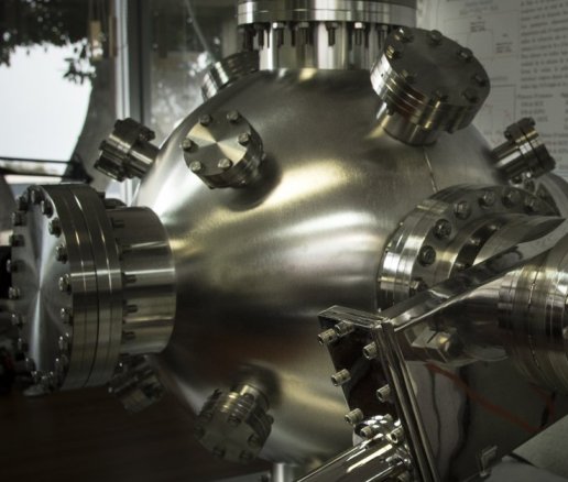
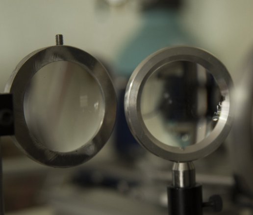
Facilities
State of the art technology for thin film deposition, spectroscopic analysis, and laser ablation. Technical information about the ellipsometers, spectrometers, lasers, AFM Park System machines, and thin film deposition equipment available at SAOMLab.